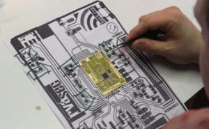
Paul Bruggeman from HackRVA provided us with an update on the badges!
Badge Design

The printed circuit board, or PCB, is the backbone of any circuit board. It supplies the physical strength and fundamental wiring for the board. It also determines the minimum size.
The circuit design artwork is  drawn, usually with special software but hobbyists sometimes just draw them by hand. The gEDA software suite has a component called “pcb” that was used to draw the badge.
Badge Etching

The PCB board is fiberglass-reinforced epoxy laminated with a thin copper sheet which is etched away using ferric chloride to recreate the artwork.
One goal of this year’s badge was to use a professional process to cover the  boards with the acid resist. Attempts last year worked but were not consistent.
Badge Cutting

Once the boards are etched they have to be cut down to final size. PCBs are tough material to cut.
The addition of a sheet metal cutter this year has made it much easier to do. The steel blade is 1/2″ thick and the whole thing weighs 60 lbs!
Badge Parts

With the boards cut down, the next process is to put the surface mount parts on. Most of the 50+ parts are surface mount. This means they have no wires to solder, because they have metals pads that melt and attach when heated to 510F degrees.
The process of installing the parts is called “pick and place.” Not very  complicated, but it can be tedious to do, especially 350 times!
Badge pick+place
 First a solder paste containing thousands of beads of tin is drawn across a stencil that leaves the sticky grey paste where the parts will be placed. This stencil is etched copper foil. Stencils can also be plastic or steel.
The board then makes its way down the volunteer assembly line where parts  are carefully placed on the solder paste. We have had the help of over a dozen HackRVA people so far this year.
Badge Cooking
 The solder paste has to be melted or “re-flowed” to electrically connect the parts to the PCB. This currently is not very hi-tech: $20 donated ovens. A volunteer last year built a micro- controlled unit but the heating element died on it.
The manual ovens require attention. Failures are usually of the distracted  human type. We had a board last year survive a 5-hour session underneath the oven, and it worked fine–though it looked like burnt toast!
Badge Wrap-up

The last things to go on are the hand- soldered parts: infrared transmitter and receiver, piezo buzzer, USB connector, USB detection wire, and the LCD panel.
If you plan on doing any software development we recommend the reset  button option (red in picture) which can be soldered across the middle and far right pin on the lower center 5-pin programming header.
Design: Paul, Morgan
Electronics: Paul
Coordinator: Morgan
Etch: Paul, Jon, Aaron
Pick+place: Jon, John, Bill, John, Yijie, Sidney,
Thad, Tony (so far)
